Comparative Study of the Device Parameters of Schottky Barrier Solar Cells and Homo-Heterojunction Solar Cells
DOI:
https://doi.org/10.54117/ijps.v2i2.18Keywords:
n – n – p Homo-heterojunction Solar Cells, n – n Schottky Barrier Solar Cells, Non – linear Response, Rectifying Response, EfficiencyAbstract
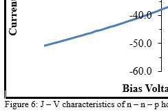
This paper reports how the p – CdTe layers grown on Schottky heterostructure influences the opto-electronic behaviour of homo-heterojunction solar cell devices fabricated from CdTe – based device architecture. Two sets of device architecture namely n – n Schottky barrier solar cells and homo-heterojunction – based solar cells with n – n – p device structure was investigated. Schottky barrier solar cells were fabricated using glass/FTO/n – CdS/n – CdTe/Au device structure and this serves as the baseline for comparison with the homo-heterojunction solar cells having p – CdTe layers. The multijunction-based homo-heterojunction solar cells with the n – n – p device architecture was fabricated using glass/FTO/n – CdS/n – CdTe/p – CdTe/Au. The p – CdTe layers grown on n – CdTe affect the solar cell and diode current – voltage characteristics, hence influencing the device electronic parameters. Non – linear and rectifying responses were observed for homo-heterojunction solar cells and n – n Schottky barrier solar cells respectively, when measured under dark condition. Under illumination condition, the cell parameters of the homo-heterojunction solar cells improved as compared to the Schottky barrier solar cells. Short circuit current density values of 27.0 mAcm-2 and 38.0 mAcm-2 were obtained for the Schottky barrier and homo-heterojunction – based solar cells respectively. Overall, higher efficiency values of ~4.91% and 7.39% were obtained for the Schottky barrier and homo-heterojunction – based solar cells respectively. Some of the electronic parameters influenced by the insertion of p – CdTe layers on the Schottky heterostructure are: leakage currents, potential barrier heights, ideality factor, series resistance and shunt resistance; the detailed results of these electronic parameters are presented in this article.
Downloads
Published
How to Cite
Issue
Section
License
Copyright (c) 2025 O. I. Olusola, N. E. Adesiji, A. F. Afolabi, O. O. Olusola, J. A. Adedeji, P. O. Elujoba, S. S. Oluyamo

This work is licensed under a Creative Commons Attribution 4.0 International License.
